Product Features
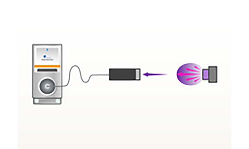
:: Non-contact, non-destructive, measuring heads can be freely integrated into the customer's system
● A beginner's parsing model that can be easily parsed by beginners.
:: Highly accurate and reproducible measurement of absolute reflectance in the ultraviolet to near-infrared wavelength bands, with the ability to analyze the thickness of multilayer films and optical constants (n: refractive index, k: extinction coefficient)
● Single-point focus and measurement in less than 1 second
:: Wide range of optical systems (UV ~ NIR) for microscopic spectroscopy
● Individual test heads for various inline customization needs
● The smallest corresponding spot is about 3μm.
:: Exclusive patent for resolving nk for ultra-thin films
Measurement items
● Absolute reflectance analysis
:: Multilayer film analysis (50 layers)
● Optical constants (n: refractive index, k: extinction coefficient)
In the case of transparent substrate samples such as film or glass, which cannot be measured correctly due to internal reflections from the substrate, the OPTM series uses an objective lens that physically removes internal reflections, enabling high-precision measurements to be made even on transparent substrates. In addition, samples such as films or SiC with optical anisotropy can be measured independently of their influence.
(Patent No. 5172203)

Scope of Application
:: Semiconductors, compound semiconductors: silicon semiconductors, silicon carbide semiconductors, gallium arsenide semiconductors, photoresists, dielectric constant materials
:: FPD: LCD, TFT, OLED (organic EL)
:: Data storage: DVDs, magnetic head film, magnetic materials
:: Optical materials: filters, anti-reflective films
:: Flat panel displays: liquid crystal displays, thin film transistors, OLEDs
● Films: AR film, HC film, PET film, etc.
:: Others: construction materials, glue, DLC, etc.
specification
(Automatic XY platform type)
| OPTM-A1 | OPTM-A2 | OPTM-A3 | |
|---|---|---|---|
| wavelength range | 230 ~ 800 nm | 360 ~ 1100 nm | 900 ~ 1600 nm |
| Film thickness range | 1nm ~ 35μm | 7nm ~ 49μm | 16nm ~ 92μm |
| measuring time | 1 second / within 1 point | ||
| Aperture size | 10μm (min. approx. 3μm) | ||
| sensor | CCD | InGaAs | |
| Light source specifications | Deuterium + halogen lamps | halogen lamp | |
| sizes | 556(W) X 566(D) X 618(H) mm (main part of automatic XY platform type) | ||
| weights | 66kg (main part of automatic XY platform type) | ||
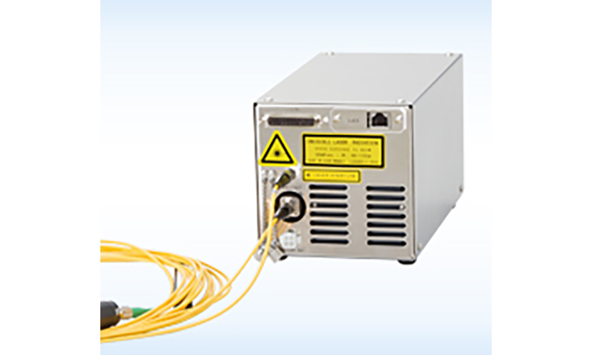
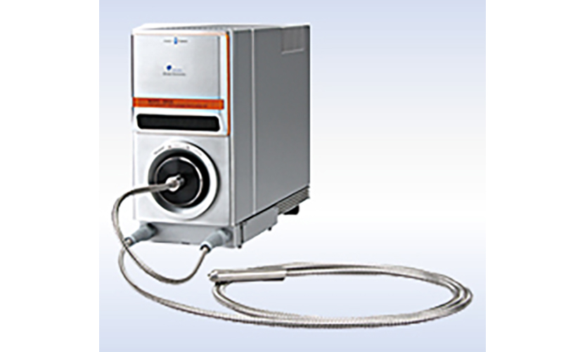
OPTM Selection
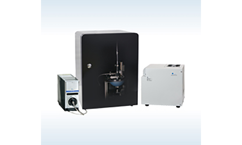
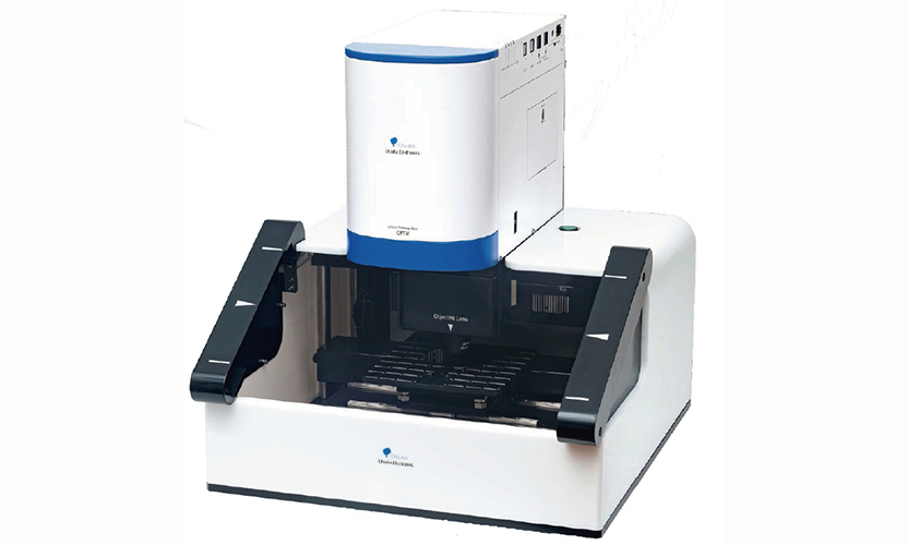
 Automatic XY platform type
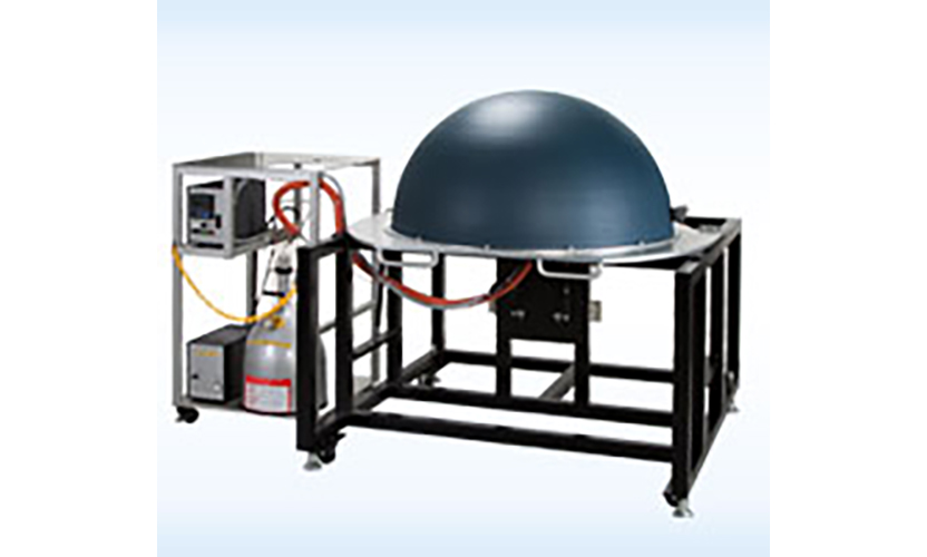
 Fixed frame type
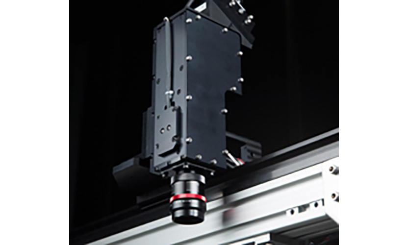
 Embedded Head Shape
Wavelength and film thickness range

Selection table
| wavelength range | Automatic XY platform type | Fixed frame type | Embedded Head Shape |
| 230 ~ 800nm | OPTM-A1 | OPTM-F1 | OPTM-H1 |
| 360 ~ 1,100nm | OPTM-A2 | OPTM-F2 | OPTM-H2 |
| 900 ~ 1,600nm | OPTM-A3 | OPTM-F3 | OPTM-H3 |
objective (optics)
| typology | magnification | Measuring the spot | field of view |
| reflecting pair | 10x lens | Φ 20μm | Φ 800μm |
| 20x lens | Φ 10μm | Φ 400μm | |
| 40x lens | Φ 5μm | Φ 200μm | |
| Visual Refractive | 5x lens | Φ 40μm | Φ 1,600μm |
Measurement Cases
Semiconductor Industry - SiO2, SiN Film Thickness Measurement Cases

In semiconductor processes, SiO2 is used as an insulating film, while SiN is used as an insulating film with a higher dielectric constant than SiO2, or as a blocking protection when SiO2 is removed by CMP, after which SiN is also removed. When the properties of insulating films are used in this way, it is necessary to measure the thickness of these films for accurate process control.
FPD Industry - Color Photoresist Film Thickness Measurement


In the production process of color filter film, the color photoresist is generally coated on the entire glass surface, and the desired pattern is left by photolithography for exposure and development.RGB three colors in turn to complete this process.
The non-constant thickness of color photoresist is the cause of deformation of RGB patterns and color deviation of color filters, so it is very important to manage the film thickness of color photoresist.
FPD Industry - Analyzing ITO Construction with Tilt Mode


ITO film is a transparent electrode material used in liquid crystal panels and other applications, and is annealed (heat-treated) to improve conductivity and light transmittance after film production. At this time, the oxygen state and crystallinity change, causing the film thickness to change in a staged tilt. Optically, the film cannot be regarded as a homogeneous single-layer film.
The degree of tilt is measured from the nk values of the upper and lower interfaces using the tilt mode for such an ITO.
Semiconductor Industry - Determination of Film Thickness on Rough Substrates Using Interface Coefficients


If the surface of the substrate is non-specular and rough, the measured light is reduced due to scattering and the measured reflectance is lower than the actual value.
By using the interfacial coefficient, the value of the film thickness of the film on the substrate can be measured because it takes into account the reduction of the reflectivity on the substrate surface.
DLC Coating Industry - Measurement of DLC Coating Thickness for Various Applications

DLC (diamond-like) coatings are used in a wide variety of applications due to their high hardness, low coefficient of friction, abrasion resistance, electrical insulation, high barrier properties, surface modification, and affinity with other materials.
The micro-optical system enables measurement of shaped samples. In addition, the monitor can be used to analyze the cause of anomalies by checking the measurement position and measuring at the same time.