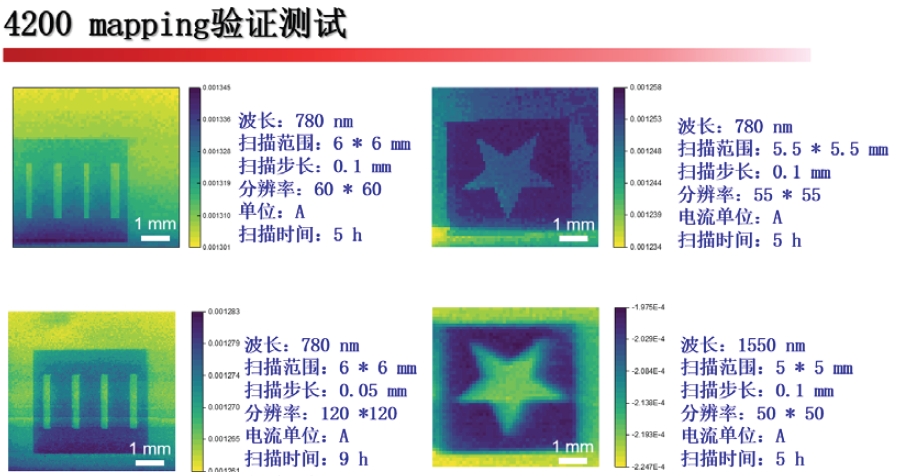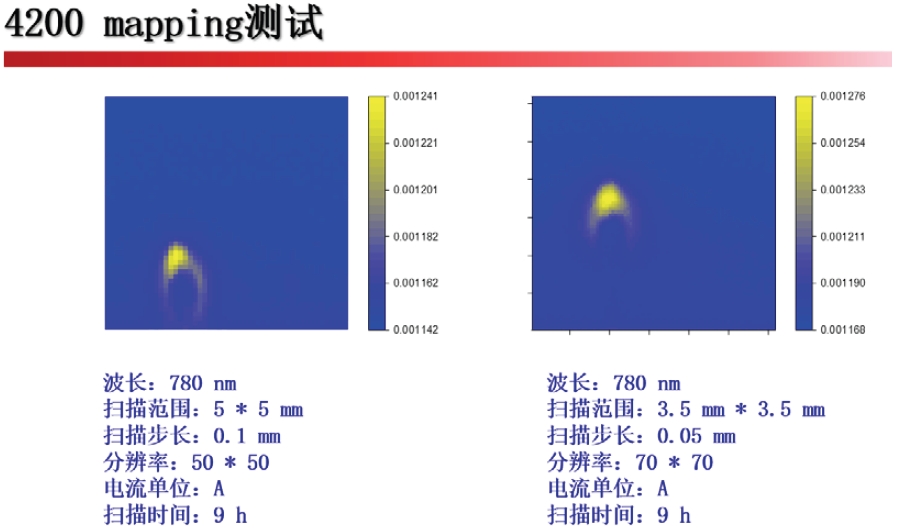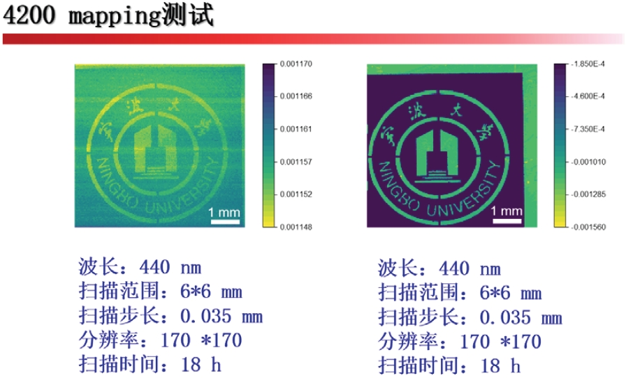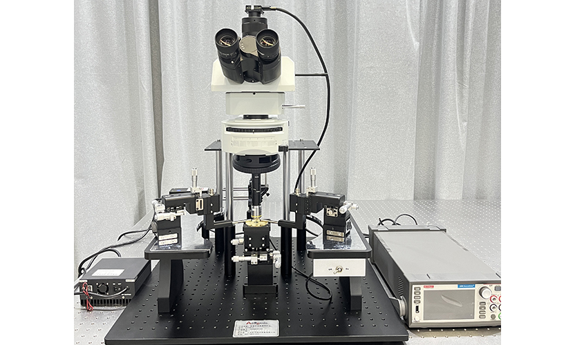
Micro-nano optoelectronic imaging test system is a kind of micro-imaging means, through different wavelengths of laser detection, analysis and characterization of optoelectronic devices, such as short-circuit current distribution, surface defects, reflectivity and other parameters. And through the scanning of the images obtained to analyze the uniformity of various parameters of the plane, for optoelectronic device structure optimization to provide reference. The laser pass is focused onto the sample surface by the microscope, the laser excites the sample to generate photocurrent, and the photocurrent signal is led out to the current source meter through the probe, and then read out by the software. During scanning, the laser spot moves in the XY direction of the sample through the movement of the motorized displacement stage. The software records the position of each focused laser spot and its corresponding current value, and synchronously depicts the photocurrent imaging map on the software, which shows the current distribution of the sample.
Technical Parameters
| Lasers (light sources) | Standard 532nm laser, energy stability 1%@4hours |
| Microscope Module | Reflective/Transmissive LED Lighting
Objective: Standard (20X, WD=7.5mm) Extra long working distance Maximum scanning range: 260 x 200 μm (at 20x objective) Position repeatability: less than 1 μm Minimum scanning step: 0.2μm Laser spot: 2μm |
| data acquisition | Current source meter: Keithley 2450
Measurement range: 1nA ・ 1A Dark noise: 50pA Resolution: 20fA |
| Probe Station Module | 65mm diameter vacuum chuck 2D movement of probe holder and sample as a whole, 2D movement of sample position alone, 25mm sample position travel, 5μm resolution Probe holder: XYZ travel 12mm, 0.7μm resolution Probe: tungsten needles, 5μm, 10μm, 20μm diameter selectable |
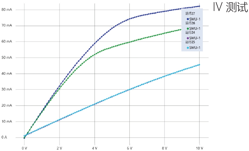
| hardware | Optical current scanning (Mapping): you can set a fixed voltage, point by point to obtain the current value
I-V curve scanning (Mapping): You can set the specified voltage interval to obtain I-V curve point by point Specified area scanning (Mapping) |
| Spectral responsivity test (optional) | Spectral range 200-1100nm, extendable to 2500nm
Spectral responsivity curve Quantum efficiency curve Bias setting function |
| Laser (option) | Wavelength: 405nm or 635nm optional, other wavelengths consulting sales
Energy stability: less than 1% @ 2 hours Power: 10mW and 30mW (optional) |
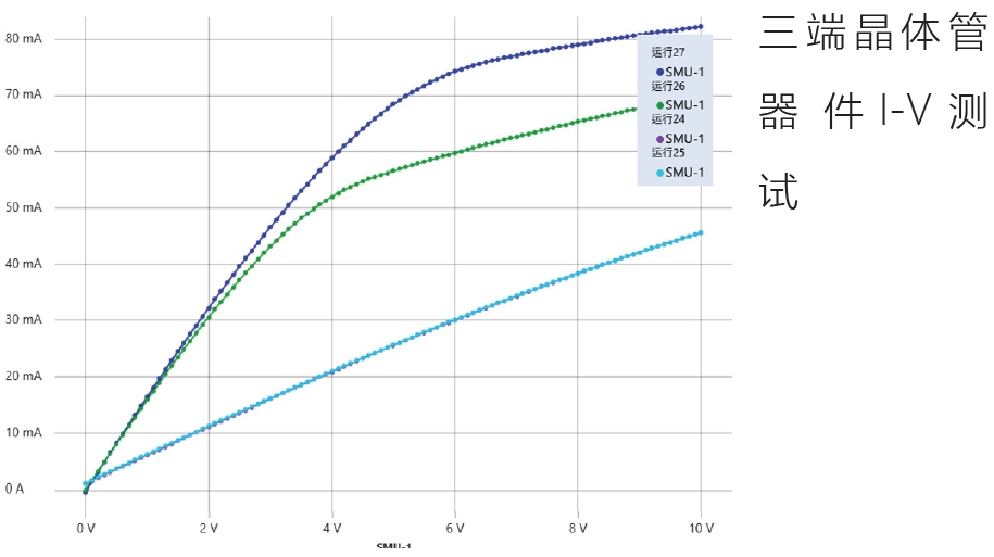
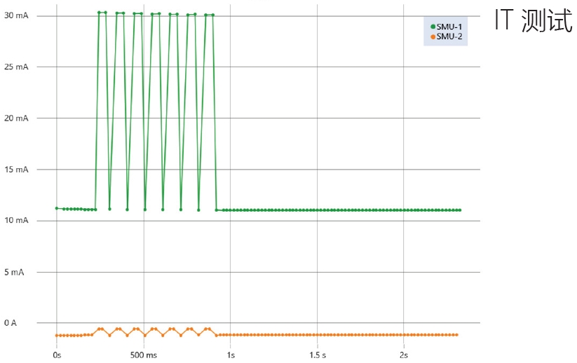
Test case: