Electrostatic Interactions in Wafer Processes and Semiconductor Technology

Discover the mysteries of wafer fabrication!
Semiconductor industry friends, do you want to understand the electrostatic interaction between wafers and lapping solutions in the process? Are you eager to master the latest semiconductor process technology? Otsuka Electronics will hold a webinar on July 24, 2024, 15:00-16:00, with the theme of "Evaluation Methods of Electrostatic Interaction between Wafers and Milling Fluids and Introduction to Semiconductor Process Technology", and invites you to join us for a discussion and exchange of ideas.

This seminar is dedicated to professionals and research organizations in the following fields:

  • abrasive
  • Semiconductor grinding process
  • CMP and BG equipment vendors
  • Temporary bonding and etching process
  • Semiconductor Defect Detection
POMINCO Instruments Cooperative Promotion
As a long-term partner of Otsuka Electronics, Shanghai POMIN Scientific Instruments Co., Ltd. will strongly support and publicize this seminar. At the same time, we will also highlight four core products, which will be demonstrated in detail at the seminar, bringing you a technical feast.

1 Light-wave field three-dimensional microscopy MINUK
The MINUK Lightwave Field 3D Microscope enables high-precision, high-resolution 3D imaging, providing powerful support for microscopic analysis in semiconductor processes.

2 ZETA Potential - Particle Size - Molecular Weight Testing System ELSZNEO
The ELSZNEO test system accurately measures zeta potential, particle size and molecular weight to help you gain insight into the properties of your grinding fluids and their performance in different processes.

3 Spectral Interference Wafer Thickness Gauge SF-3
SF-3 Spectral Interferometer Wafer Thickness GaugeProvides you with accurate film thickness measurements, an indispensable tool in the semiconductor manufacturing process.

4 Microscopic spectrophotometer OPTM SERIES
OPTM series microspectral filmThickness gauges that realize precise measurement of film thickness through microspectroscopic spectroscopy, helping semiconductor processes to be carried out efficiently.

Participation
It's easy and fast to attend, just scan the QR code and submit your application to attend the conference for free. This is a rare opportunity to learn about the latest technology, exchange industry experience, and discuss with industry experts face-to-face.

Scan the QR code below to apply for the conference now and explore the mysteries of wafer processing with Otsuka Electronics! If your application is approved, you will receive an email with a link to the conference on the day of the conference.

Meeting time: 2024July 24, 2011, 15:00-16:00

Otsuka Electronics and ShanghaiWe are looking forward to your participation to witness the latest advances in semiconductor process technology!

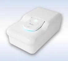
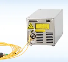
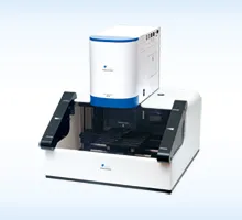
# Otsuka Electronics # Webinar # Wafer Processing # Semiconductor Technology # Electrostatic Interactions # Free Attendance # Shanghai POMIN Scientific Instruments #MINUK #ELSZNEO #SF-3 #OPTM

Please share this article in your circle of friends and workgroups, so that more colleagues can participate in this event and jointly promote the development of semiconductor technology!

Hello, please contact us with any questions!
en_USEnglish